- 您现在的位置:买卖IC网 > Sheet目录313 > AT45DB081B-TI (Atmel)IC FLASH 8MBIT 20MHZ 28TSOP
�� �
�
�Successive� page� programming� operations� without� doing� a� page� erase� are� not� recommended.� In�
�other� words,� changing� bytes� within� a� page� from� a� “1”� to� a� “0”� during� multiple� page� programming�
�operations� without� erasing� that� page� is� not� recommended.�
�PAGE� ERASE:� The� optional� Page� Erase� command� can� be� used� to� individually� erase� any� page�
�in� the� main� memory� array� allowing� the� Buffer� to� Main� Memory� Page� Program� without� Built-in�
�Erase� command� to� be� utilized� at� a� later� time.� To� perform� a� Page� Erase,� an� opcode� of� 81H� must�
�be� loaded� into� the� device,� followed� by� three� reserved� bits,� 12� address� bits� (PA11� -� PA0),� and�
�nine� don’t� care� bits.� The� 12� address� bits� are� used� to� specify� which� page� of� the� memory� array� is�
�to� be� erased.� When� a� low-to-high� transition� occurs� on� the� CS� pin,� the� part� will� erase� the� selected�
�page� to� 1s.� The� erase� operation� is� internally� self-timed� and� should� take� place� in� a� maximum� time�
�of� t� PE� .� During� this� time,� the� status� register� will� indicate� that� the� part� is� busy.�
�BLOCK� ERASE:� A� block� of� eight� pages� can� be� erased� at� one� time� allowing� the� Buffer� to� Main�
�Memory� Page� Program� without� Built-in� Erase� command� to� be� utilized� to� reduce� programming�
�times� when� writing� large� amounts� of� data� to� the� device.� To� perform� a� Block� Erase,� an� opcode� of�
�50H� must� be� loaded� into� the� device,� followed� by� three� reserved� bits,� nine� address� bits� (PA11� -�
�PA3),� and� 12� don’t� care� bits.� The� nine� address� bits� are� used� to� specify� which� block� of� eight�
�pages� is� to� be� erased.� When� a� low-to-high� transition� occurs� on� the� CS� pin,� the� part� will� erase� the�
�selected� block� of� eight� pages� to� 1s.� The� erase� operation� is� internally� self-timed� and� should� take�
�place� in� a� maximum� time� of� t� BE� .� During� this� time,� the� status� register� will� indicate� that� the� part� is�
�busy.�
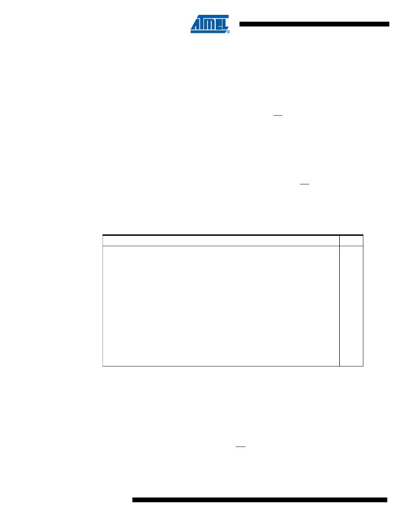
�Block� Erase� Addressing�
�PA11�
�0�
�0�
�0�
�0�
�?�
�?�
�?�
�1�
�1�
�1�
�1�
�PA10�
�0�
�0�
�0�
�0�
�?�
�?�
�?�
�1�
�1�
�1�
�1�
�PA9�
�0�
�0�
�0�
�0�
�?�
�?�
�?�
�1�
�1�
�1�
�1�
�PA8�
�0�
�0�
�0�
�0�
�?�
�?�
�?�
�1�
�1�
�1�
�1�
�PA7�
�0�
�0�
�0�
�0�
�?�
�?�
�?�
�1�
�1�
�1�
�1�
�PA6�
�0�
�0�
�0�
�0�
�?�
�?�
�?�
�1�
�1�
�1�
�1�
�PA5�
�0�
�0�
�0�
�0�
�?�
�?�
�?�
�1�
�1�
�1�
�1�
�PA4�
�0�
�0�
�1�
�1�
�?�
�?�
�?�
�0�
�0�
�1�
�1�
�PA3�
�0�
�1�
�0�
�1�
�?�
�?�
�?�
�0�
�1�
�0�
�1�
�PA2�
�X�
�X�
�X�
�X�
�?�
�?�
�?�
�X�
�X�
�X�
�X�
�PA1�
�X�
�X�
�X�
�X�
�?�
�?�
�?�
�X�
�X�
�X�
�X�
�PA0�
�X�
�X�
�X�
�X�
�?�
�?�
�?�
�X�
�X�
�X�
�X�
�Block�
�0�
�1�
�2�
�3�
�?�
�?�
�?�
�508�
�509�
�510�
�511�
�MAIN� MEMORY� PAGE� PROGRAM� THROUGH� BUFFER:� This� operation� is� a� combination� of� the�
�Buffer� Write� and� Buffer� to� Main� Memory� Page� Program� with� Built-in� Erase� operations.� Data� is�
�first� shifted� into� buffer� 1� or� buffer� 2� from� the� SI� pin� and� then� programmed� into� a� specified� page� in�
�the� main� memory.� To� initiate� the� operation,� an� 8-bit� opcode,� 82H� for� buffer� 1� or� 85H� for� buffer� 2,�
�must� be� followed� by� the� three� reserved� bits� and� 21� address� bits.� The� 12� most� significant� address�
�bits� (PA11� -� PA0)� select� the� page� in� the� main� memory� where� data� is� to� be� written,� and� the� next�
�nine� address� bits� (BFA8� -� BFA0)� select� the� first� byte� in� the� buffer� to� be� written.� After� all� address�
�bits� are� shifted� in,� the� part� will� take� data� from� the� SI� pin� and� store� it� in� one� of� the� data� buffers.� If�
�the� end� of� the� buffer� is� reached,� the� device� will� wrap� around� back� to� the� beginning� of� the� buffer.�
�When� there� is� a� low-to-high� transition� on� the� CS� pin,� the� part� will� first� erase� the� selected� page� in�
�main� memory� to� all� 1s� and� then� program� the� data� stored� in� the� buffer� into� the� specified� page� in�
�the� main� memory.� Both� the� erase� and� the� programming� of� the� page� are� internally� self-timed� and�
�6�
�AT45DB081B�
�2225J–DFLSH–2/08�
�发布紧急采购,3分钟左右您将得到回复。
相关PDF资料
AT45DB161B-TI
IC FLASH 16MBIT 20MHZ 28TSOP
AT45DB321-TC
IC FLASH 32MBIT 13MHZ 32TSOP
AT45DB321B-TI
IC FLASH 32MBIT 20MHZ 32TSOP
AT45DB321C-TC
IC FLASH 32MBIT 40MHZ 28TSOP
AT45DB642-TC
IC FLASH 64MBIT 20MHZ 40TSOP
AT88CK9000-8TH
CRYPTO PROGRAMMER BOARD 8-TSSOP
AT88SC12816C-MJ
IC EEPROM 128KBIT 1.5MHZ M2J
AT88SC25616C-MJ
IC EEPROM 256BIT 1.5MHZ M2J
相关代理商/技术参数
AT45DB081B-TI-2.5
功能描述:闪存 8M SERIAL 2.7V - 2.5V IND TEMP RoHS:否 制造商:ON Semiconductor 数据总线宽度:1 bit 存储类型:Flash 存储容量:2 MB 结构:256 K x 8 定时类型: 接口类型:SPI 访问时间: 电源电压-最大:3.6 V 电源电压-最小:2.3 V 最大工作电流:15 mA 工作温度:- 40 C to + 85 C 安装风格:SMD/SMT 封装 / 箱体: 封装:Reel
AT45DB081B-TU
功能描述:闪存 8M 28 I/O Pins SPI 264B 2.7V RoHS:否 制造商:ON Semiconductor 数据总线宽度:1 bit 存储类型:Flash 存储容量:2 MB 结构:256 K x 8 定时类型: 接口类型:SPI 访问时间: 电源电压-最大:3.6 V 电源电压-最小:2.3 V 最大工作电流:15 mA 工作温度:- 40 C to + 85 C 安装风格:SMD/SMT 封装 / 箱体: 封装:Reel
AT45DB081D
制造商:ATMEL 制造商全称:ATMEL Corporation 功能描述:8-megabit 2.5-volt or 2.7-volt DataFlash
AT45DB081D_07
制造商:ATMEL 制造商全称:ATMEL Corporation 功能描述:8-megabit 2.5-volt or 2.7-volt DataFlash
AT45DB081D_08
制造商:ATMEL 制造商全称:ATMEL Corporation 功能描述:8-megabit 2.5-volt or 2.7-volt DataFlash
AT45DB081D_09
制造商:ATMEL 制造商全称:ATMEL Corporation 功能描述:8-megabit 2.5-volt or 2.7-volt DataFlash
AT45DB081D_13
制造商:AD 制造商全称:Analog Devices 功能描述:8-megabit 2.5V or 2.7V DataFlash
AT45DB081D-DWF
制造商:Adesto Technologies Corporation 功能描述:WHOLE WAFER, NO BACKGRIND - Gel-pak, waffle pack, wafer, diced wafer on film